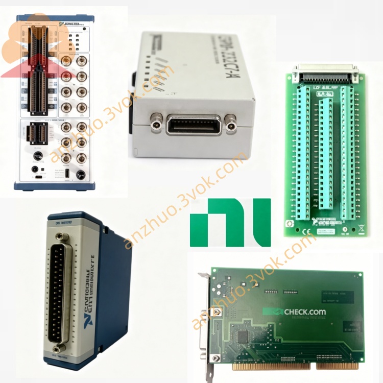
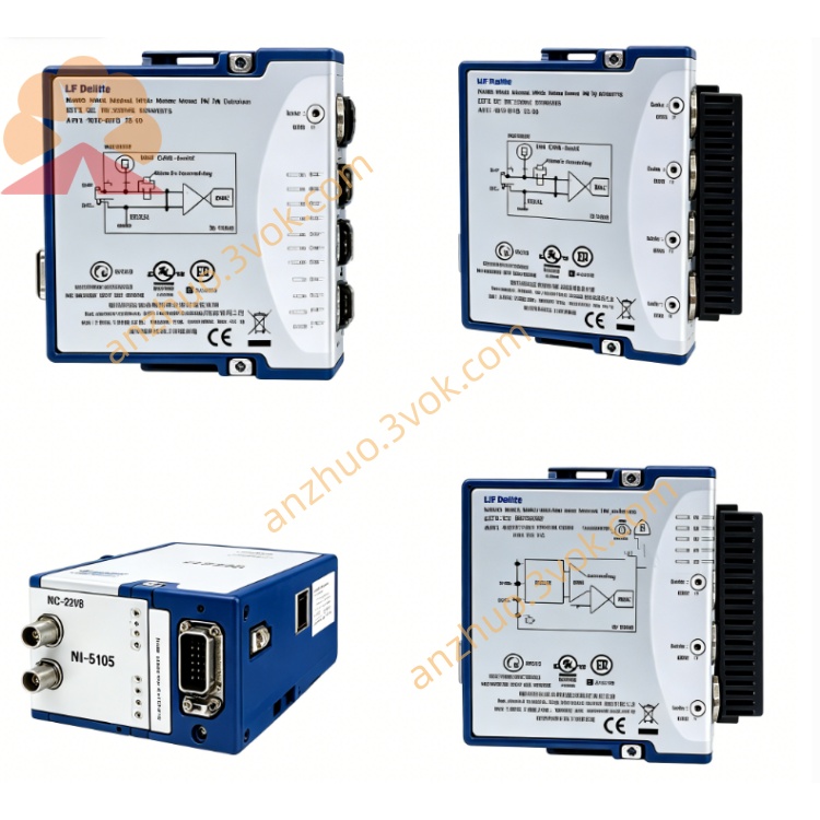
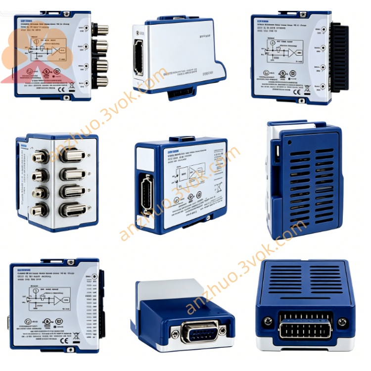
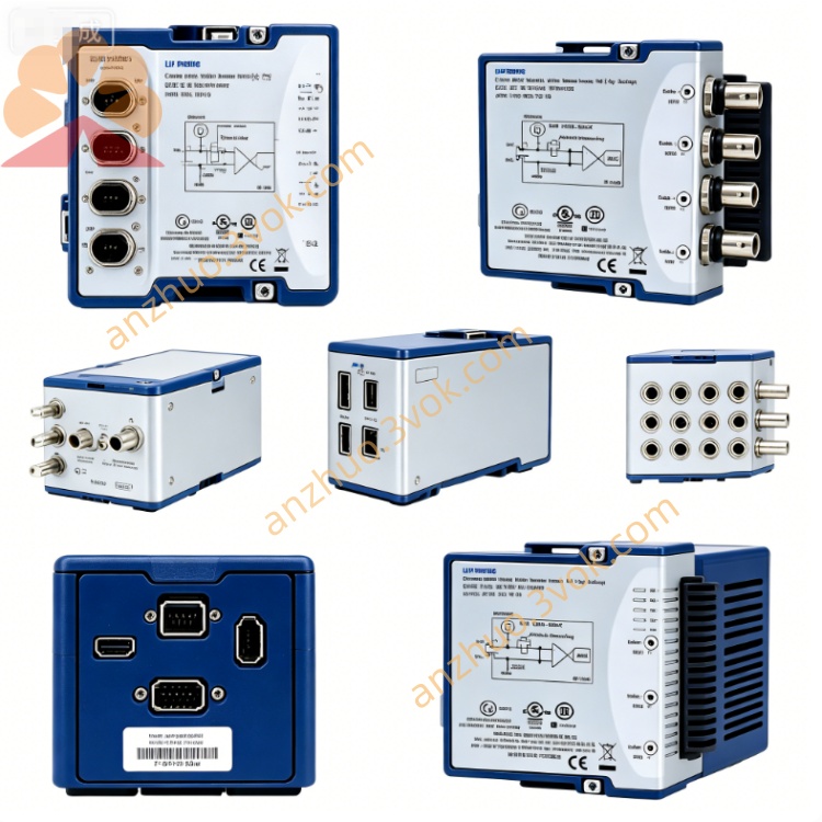
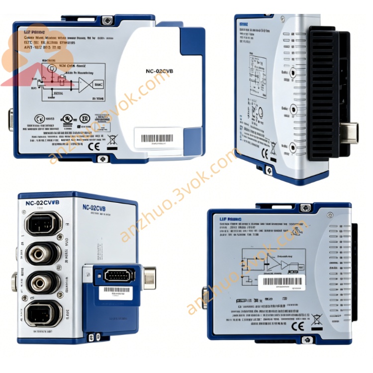
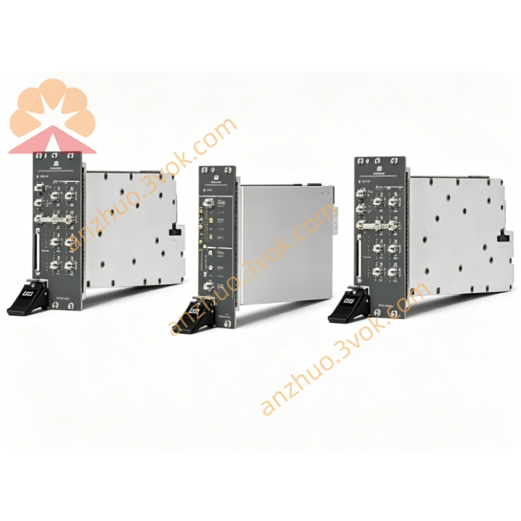
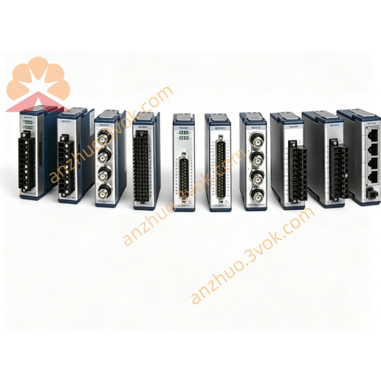
PCI-7811R
Description
Main technical parameters (simplified)
1. FPGA core
Model: Virtex-II XC2V1000 (1M logic gates)
Resources: 10,240 flip-flops, 40×18×18 multipliers, 720 Kbit block RAM
Development: LabVIEW FPGA graphical programming, hardware execution
2. Digital I/O (DIO)
Number of channels: 160 bidirectional DIO (can be configured as input/output arbitrarily)
Channel rate: Up to 40 MHz (hardware timing)
Function configuration:
Digital input/output (TTL level)
32-bit counter/timer, PWM output
Encoder A/B/Z phase input (up to 40 MHz)
Custom serial protocols (SPI, UART, etc.)
Isolation: I/O isolated from the chassis at 2500 Vrms, strong anti-interference
3. Synchronization and storage
Synchronization bus: RTSI (8 channels of trigger + 1 channel of clock, multi-card synchronization)
On-board cache: 80 KB FIFO, supports DMA streaming data
FPGA RAM: 720 Kbit block RAM (user available)
4. Electrical and environmental
Power supply: +3.3 V @ 650 mA; +5 V @ 9 mA
Power consumption: Approximately 2.2 W
Operating temperature: 0 - 55 °C (standard); -40 - 85 °C (extended temperature version)
Size: Standard half-length PCI (170 × 109 mm)
5. Typical Applications
High-speed digital I/O control: Industrial automation, semiconductor testing, electronic manufacturing
Hardware-in-the-Loop (HIL) testing: Control algorithm verification, real-time simulation
Custom timing/triggers: Synchronous sampling, pulse sequence generation, precise timing
Motion control: High-speed pulse output, encoder acquisition, multi-axis synchronization
Communication protocols: Custom serial ports, parallel interfaces, dedicated buses
Get a Quote